Monday, September 30, 2013

Petrol Gas Switch For A Pajero

My current vehicle, a Pajero, was modified for dual fuel - ie, petrol and gas. However, its necessary to run the vehicle on petrol at regular intervals to stop the injectors from clogging up. This simple circuit allows the vehicle to be started using petrol and then automatically switches it to gas when the speed exceeds 45km/h and the brake pedal is pressed. Alternatively, the vehicle may be run on petrol simply by switching the existing petrol/gas switch to petrol.

You can also start the vehicle on gas by pressing the brake pedal while starting the vehicle. The circuit is based on an LM324 dual op amp, with both op amps wired as comparators. It works like this: IC1a buffers the signal from the vehicles speed sensor and drives an output filter network (D1, a 560kO resistor and a 10µF capacitor) to produce a DC voltage thats proportional to the vehicles speed.

Circuit diagram:

petrol-gas-switch-for-a-pajero

Petrol Gas Switch For A Pajero Circuit diagram

This voltage is then applied to pin 5 of IC1b and compared with the voltage set by trimpot VR1. When pin 7 of IC1b goes high, transistor Q1 turns on. This also turns on transistor Q2 when the brake pedal is pressed (pressing the brake pedal applies +12V from the brake light circuit to Q2s emitter). And when Q2 turns on, relay 1 turns on and its contacts switch to the gas position. Trimpot VR1 must be adjusted so that IC1bs pin 7 output switches high when the desired trigger speed is reached (ie, 45km/h). In effect, the speed signal is ANDed with the brake light signal to turn on the relay. The vehicle has been running this circuit for several years now and is still running well, with no further injector cleans required.

Author: J. Malnar - Copyright: Silicon Chip Electronics

Continue Reading..

Sunday, September 29, 2013

Neon Flasher Runs From 3V Supply

A neon indicator typically requires at least 70V to fire it and normally would not be contemplated in a battery circuit. However, this little switchmode circuit from the Linear Technology website (www.linear-tech.com) steps up the 3V battery supply to around 95V or so, to drive a neon with ease. The circuit has two parts: IC1 operating as step-up converter at around 75kHz and a diode pump, consisting of three 1N4148 diodes and associated .022µF capacitors. The 3.3MO resistor and the 0.68µF capacitor set the flashing rate to about once every two seconds. The average DC level from the diode pump is set to about 95V by the 100MO feedback resistor to pin 8. The circuit could also use an LT1111 (RS Components Cat 217-0448) which would run at about 20kHz so L1 could be reduced to 100mH and use a powdered iron toroid core from Neosid or Jaycar.

neon flasher circuit schematic
Continue Reading..

Saturday, September 28, 2013

Modular Phono Preamplifier


High Quality Moving Magnet Pick-up module
Two-stage Series/Shunt feedback RIAA equalization


Any electronics amateur still in possess of a collection of vinyl recordings and aiming at a high quality reproduction should build this preamp and add it to the Modular Preamplifier chain. This circuit features a very high input overload capability, very low distortion and accurate reproduction of the RIAA equalization curve, thanks to a two-stage op-amp circuitry in which the RIAA equalization network was split in two halves: an input stage (IC1A) wired in a series feedback configuration, implementing the bass-boost part of the RIAA equalization curve and a second stage, implementing the treble-cut part of the curve by means of a second op-amp (IC2A) wired in the shunt feedback configuration.

Modular Phono Preamplifier circuit diagramParts:

R1_____________270R 1/4W Resistor
R2_____________100K 1/4W Resistor
R3_______________2K2 1/4W Resistor
R4______________39K 1/4W Resistor
R5_______________3K9 1/4W Resistor
R6_____________390K 1/4W Resistor
R7______________33K 1/4W Resistor
R8______________75K 1/4W Resistor (or two 150K resistors wired in parallel)
R9_____________560R 1/4W Resistor
C1_____________220pF 63V Polystyrene or Ceramic Capacitor
C2_______________1µF 63V Polyester Capacitor
C3______________47µF 25V Electrolytic Capacitor
C4______________10nF 63V Polyester Capacitor 5% tolerance or better
C5_______________1nF 63V Polyester Capacitor 5% tolerance or better
C6,C9__________100nF 63V Polyester Capacitors
C7,C10__________22µF 25V Electrolytic Capacitors
C8,C11________2200µF 25V Electrolytic Capacitors
IC1___________LM833 or NE5532 Low noise Dual Op-amp
IC2___________TL072 Dual BIFET Op-Amp
IC3___________78L15 15V 100mA Positive Regulator IC
IC4___________79L15 15V 100mA Negative Regulator IC
D1,D2________1N4002 200V 1A Diodes
J1,J2___________RCA audio input sockets
J3______________Mini DC Power Socket

This module comprises also an independent dual rail power supply identical to that described in the Modular Preamplifier Control Center. As with the other modules of this series, each electronic board can be fitted into a standard enclosure: Hammond extruded aluminum cases are well suited to host the boards of this preamp. In particular, the cases sized 16 x 10.3 x 5.3 cm or 22 x 10.3 x 5.3 cm have a very good look when stacked. See below an example of the possible arrangement of the rear panel of this module.

Notes:
  • The circuit diagram shows the Left channel only and the power supply
  • Some parts are in common to both channels and must not be doubled. These parts are: IC3, IC4, C6, C7, C8, C9, C10, C11, D1, D2 and J3.
  • IC1 and IC2 are dual Op-Amps, therefore the second half of these devices will be used for the Right channel
  • This module requires an external 15 - 18V ac (50mA minimum) Power Supply Adaptor.
Technical data:

Sensitivity @ 1KHz: 4.3mV RMS input for 200mV RMS output
Max. input voltage @ 100Hz: 53mV RMS
Max. input voltage @ 1KHz: 212mV RMS
Max. input voltage @ 10KHz: 477mV RMS
Frequency response @ 200mV RMS output: flat from 30Hz to 23KHz; -0.5dB @ 20Hz
Total harmonic distortion @ 1KHz and up to 8.8V RMS output: 0.0028%
Total harmonic distortion @10KHz and up to 4.4V RMS output: 0.008%
Continue Reading..

Friday, September 27, 2013

Battery Replacement Power Supply

Your childs battery toy has failed and you have to fix it. Once you have managed to get it apart, the battery compartment is not likely to be connected to the works or the batteries might have gone flat anyway. The solution is this switchable supply which is designed to replace from one to six dry cells. It is not intended to replace the batteries on a permanent basis, as in most cases this is not practical. The heart of the supply is an LM317T adjustable 3-terminal regulator and six trimpots selected by switch S1b. The other pole of the switch, S1a, is used to select taps on the transformer secondary, to minimize power dissipation in the LM317T. The table shows the trimpot settings for the six voltage outputs. Diode D1 and the 10µF capacitor and the LED provide power indication. This has the advantage of constant brightness which would not be obtained if the LED was run from the unregulated switchable DC.

Battery replacement power supply circuit schematic
Continue Reading..

Thursday, September 26, 2013

Simple 6 Input Alarm

This simple alarm circuit was designed for use in a combined garage and rumpus room. It can be assembled on Veroboard and uses just one IC plus a handful of cheap components. The circuit is based on a straightforward 555 timer circuit (IC1). This is wired as a monostable and sets the siren period which is adjustable up to about three minutes using potentiometer VR1. In operation, IC1s pin 2 input monitors the detector circuit for negative-going signals. When a switch is closed, a brief negative-going pulse is applied to pin 2 via a 10µF capacitor and its corresponding series diode (D2-D7). This triggers IC1 which switches its pin 3 output high and switches off relay RLY1 (ie, RLY1 is normally on).

Simple 6-input alarm circuit schematic

As a result, the piezo siren sounds for the duration of the monostable period. In addition, relay RLY2 is turned on via diode D9 and latches on via D10. This means that the strobe light (which is wired to the normally open contact) will continue to flash until the alarm is switched off (via the keyswitch). At the end of the monostable period, RLY1 turns off and this turns off the piezo siren. The circuit can then be retriggered by any further trigger inputs from the switches. A variety of detectors with normally open contacts can be used for the switches, including reed switches, pressure mats, IR detectors and glass breakage detectors. All switches must be open before the alarm is switched on.
Continue Reading..

Wednesday, September 25, 2013

Stepper Motor Generator

Any stepper motor can be used as a generator. In contrast to other generators, a stepper motor produces a large induced voltage even at low rotational speeds. The type used here, with a DC resistance of 2×60 Ω per winding, can generate more than 20 V when turned by hand, without any gearing. The circuit diagram for a ‘hand-cranked torch’ shows how you can use a stepper motor as a generator. A supplementary circuit stores the energy. Two bridge rectifiers, each made up of four 1N4148 diodes, charge the 4700µF capacitor. The super-bright (white) LED is driven either via a 390-Ω resistor (Power Light), or via 22 kΩ in series with 390 Ω. In the latter case, the LED is not as bright, but it stays on longer.

Stepper Motor Generator circuit diagramYou must restrain yourself when cranking the dynamo, since in the ‘bright’ setting it is possible to exceed the rated LED current of 20mA, while in the ‘long’ setting it is possible to exceed the rated capacitor voltage of 25 V. If necessary, adjust the value of the LED series resistor. The lamp is bright enough for reading in complete darkness. The stepper motor generator is thus ideal for spies, thieves and children who want to read under the bedcovers. You could also keep it handy in your hobby room, in case of a short circuit.
Continue Reading..

Tuesday, September 24, 2013

PIC Controlled Relay Driver

This circuit is a relay driver that is based on a PIC16F84A microcontroller. The board includes four relays so this lets us to control four distinct electrical devices. The controlled device may be a heater, a lamp, a computer or a motor. To use this board in the industrial area, the supply part is designed more attentively. To minimize the effects of the ac line noises, a 1:1 line filter transformer is used.

PIC-Controlled-Relay Driver Final

The transformer is a 220V to 12V, 50Hz and 3.6VA PCB type transformer. The model seen in the photo is HRDiemen E3814056. Since it is encapsulated, the transformer is isolated from the external effects. A 250V 400mA glass fuse is used to protect the circuit from damage due to excessive current. A high power device which is connected to the same line may form unwanted high amplitude signals while turning on and off. To bypass this signal effects, a variable resistor (varistor) which has a 20mm diameter is paralelly connected to the input.

 Controller-Schematic Circuit

Another protective component on the AC line is the line filter. It minimizes the noise of the line too. The connection type determines the common or differential mode filtering. The last components in the filtering part are the unpolarized 100nF 630V capacitors. When the frequency increases, the capacitive reactance (Xc) of the capacitor decreases so it has a important role in reducing the high frequency noise effects. To increase the performance, one is connected to the input and the other one is connected to the output of the filtering part.

Supply-Schematic circuit

After the filtering part, a 1A bridge diode is connected to make a full wave rectification. A 2200 uF capacitor then stabilizes the rectified signal. The PIC controller schematic is given in the project file. It contains PIC16F84A microcontroller, NPN transistors, and SPDT type relays. When a relay is energised, it draws about 40mA. As it is seen on the schematic, the relays are connected to the RB0-RB3 pins of the PIC via BC141 transistors. When the transistor gets cut off, a reverse EMF may occur and the transistor may be defected. To overcome this unwanted situation, 1N4007 diodes are connected between the supply and the transistor collectors. There are a few number of resistors in the circuit. They are all radially mounted. Example C and HEX code files are included in the project file. It energizes the next relay after every five seconds.

The components are listed below.

1 x PIC16F84A Microcontroller
1 x 220V/12V 3.6VA (or 3.2VA) PCB Type Transformer (EI 38/13.6)
1 x Line Filter (2x10mH 1:1 Transformer)
4 x 12V Relay (SPDT Type)
4 x BC141 NPN Transistor
5 x 2 Terminal PCB Terminal Block
4 x 1N4007 Diode
1 x 250V Varistor (20mm Diameter)
1 x PCB Fuse Holder
1 x 400mA Fuse
2 x 100nF/630V Unpolarized Capacitor
1 x 220uF/25V Electrolytic Capacitor
1 x 47uF/16V Electrolytic Capacitor
1 x 10uF/16V Electrolytic Capacitor
2 x 330nF/63V Unpolarized Capacitor
1 x 100nF/63V Unpolarized Capacitor
1 x 4MHz Crystal Oscillator
2 x 22pF Capacitor
1 x 18 Pin 2 Way IC Socket
4 x 820 Ohm 1/4W Resistor
1 x 1K 1/4W Resistor
1 x 4.7K 1/4W Resistor
1 x 7805 Voltage Regulator (TO220)
1 x 7812 Voltage Regulator (TO220)
1 x 1A Bridge Diode

Click here to download the schematics, PCB layouts and the code files

Source : www.extremecircuits.net

Continue Reading..

Monday, September 23, 2013

Battery Switch With Low Dropout Regulator

In the form of the LT1579 Linear Technology (www.linear-tech.com) has produced a practical battery switch with an integrated low-dropout regulator. In contrast to previous devices no diodes are required. The circuit is available in a 3.3 V version (LT1579CS8-3.3) and in a 5 V version (LT1579CS8-5), both in SO8 SMD packages. There is also an adjustable version and versions in an SO16 package which offer a greater range of control and drive signals. The main battery, whose terminal voltage must be at least 0.4 V higher than the desired output voltage, is connected to pin IN1. The backup battery is connected to pin IN2. The regulated output OUT can deliver a current of up to 300 mA. The LDO regulator part of the IC includes a pass transistor for the main input voltage IN1 and another for the backup battery on IN2.

Battery_Switch_With_LDO_Regulator_Circuit_Diagramw

The IC will switch over to the backup battery when it detects that the pass transistor for the main voltage input is in danger of no longer being able to maintain the required output voltage. The device then smoothly switches over to the backup battery. The open-drain status output BACKUP goes low to indicate when this has occurred. When neither battery is able to maintain the output voltage at the desired level the open-drain output DROPOUT goes low. The LT1579 can operate with input voltages of up to +20 V from the batteries. The regulator output OUT is short-circuit proof. The shutdown input switches off the output; if this feature is not required, the input can simply be left open.

Continue Reading..

Sunday, September 22, 2013

Mains Manager

Very often we forget to switch off the peripherals like monitor, scanner, and printer while switching off our PC. The problem is that there are separate power switches to turn the peripherals off. Normally, the peripherals are connected to a single of those four-way trailing sockets that are plugged into a single wall socket. If that socket is accessible, all the devices could be switched off from there and none of the equipment used will require any modification. Here is a mains manager circuit that allows you to turn all the equipment on or off by just operating the switch on any one of the devices; for example, when you switch off your PC, the monitor as well as other equipment will get powered down automatically.

You may choose the main equipment to control other gadgets. The main equipment is to be directly plugged into the master socket, while all other equipment are to be connected via the slave socket. The mains supply from the wall socket is to be connected to the input of the mains manager circuit. The unit operates by sensing the current drawn by the control equipment/load from the master socket. On sensing that the control equipment is on, it powers up the other (slave) sockets. The load on the master socket can be anywhere between 20 VA and 500 VA, while the load on the slave sockets can be 60 VA to 1200 VA. During the positive half cycle of the mains AC supply, diodes D4, D5, and D6 have a voltage drop of about 1.8 volts when current is drawn from the master socket.

Diode D7 carries the current during negative half cycles. Capacitor C3, in series with diode D3, is connected across the diode combination of D4 through D6, in addition to diode D7 as well as resistor R10. Thus current pulses during positive half-cycles, charge up the capacitor to 1.8 volts via diode D3. This voltage is sufficient to hold transistor T2 in forward biased condition for about 200 ms even after the controlling load on the master socket is switched off. When transistor T2 is ‘on’, transistor T1 gets forward biased and is switched on. This, in turn, triggers Triac 1, which then powers the slave loads. Capacitor C4 and resistor R9 form a snubber network to ensure that the triac turns off cleanly with an inductive load.

Mains Manager circuit schematic

LED1 indicates that the unit is operating. Capacitor C1 and zener ZD1 are effectively in series across the mains. The resulting 15V pulses across ZD1 are rectified by diode D2 and smoothened by capacitor C2 to provide the necessary DC supply for the circuit around transistors T1 and T2. Resistor R3 is used to limit the switching-on surge current, while resistor R1 serves as a bleeder for rapidly discharging capacitor C1 when the unit is unplugged. LED1 glows whenever the unit is plugged into the mains. Diode D1, in anti-parallel to LED1, carries the current during the opposite half cycles. Don’t plug anything into the master or slave sockets without testing the unit.

If possible, plug the unit into the mains via an earth leakage circuit breaker. The mains LED1 should glow and the slave LED2 should remain off. Now connect a table lamp to the master socket and switch it ‘on’. The lamp should operate as usual. The slave LED should turn ‘on’ whenever the lamp plugged into slave socket is switched on. Both lamps should be at full brightness without any flicker. If so, the unit is working correctly and can be put into use.

Note:
  1. The device connected to the master socket must have its power switch on the primary side of the internal transformer. Some electronic equipment have the power switch on the secondary side and hence these devices continue to draw a small current from the mains even when switched off. Thus such devices, if connected as the master, will not control the slave units correctly.
  2. Though this unit removes the power from the equipment being controlled, it doesn’t provide isolation from the mains. So, before working inside any equipment connected to this unit, it must be unplugged from the socket.
Continue Reading..

Saturday, September 21, 2013

Fuse Box BMW R11 Motorcycles Diagram

Fuse Box BMW R11 Motorcycles Diagram - Here are new post for Fuse Box BMW R11 Motorcycles Diagram.

Fuse Box BMW R11 Motorcycles Diagram


Fuse Box BMW R11 Motorcycles Diagram

Fuse Panel Layout Diagram Parts: Headlight, ABS, Fuel Pump, Injector, switches, tacho, Warning lamp, charge, motornic, turn/hazard, Timing Valve, lamda sensor, sidelight, brake light, Ignition Circuit, Relay, Speedo, Backlight, Starter Motor, Clutch, alarm.
Continue Reading..

Friday, September 20, 2013

2003 Ford Crown Vic Wiring Diagram

2003 Ford Crown Vic Wiring Diagram


The Part of 2003 Ford Crown Vic Wiring Diagram: auto lamp, dimmer, parking lamps, alpine, overhead console, radio, central junction box, control module, electronic cluster, main light switch, main light switch, interior, alpine.
Continue Reading..

Thursday, September 12, 2013

Regulators for Battery Powered Systems

Maxim describes various SMPS regulator topologies for battery powered systems. Isolated and non-isolated topologies are covered. This tutorial presents an overview of regulator topologies for battery-powered equipment. The discussion covers linear regulators, charge pumps, buck and boost regulators, inverters, and flyback designs. The importance of peak current is explained, and schematics of each topology are shown.


Switch mode regulators for battery powered systems 1
Continue Reading..

Wednesday, September 11, 2013

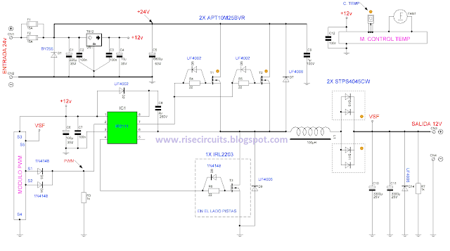
24V to 12V 400W DC Inverter Circuit

24V to 12V 400W DC Inverter Circuit Diagram
24V to 12V 400W DC Inverter Circuit

24V to 12V 20A 400W DC to DC Inverter. Does little to change my PV system 12v 24v me the problem arose of what to do with investors who already had 12V. I was looking for a pattern online and found several schemes with linear regulators 20A, this solution although quite simple, due to the huge losses they have is not advisable. Ideally, a converter switched, high-performance. At the end I found nothing I liked and decided to design my own. Circuit characteristics: Output current: 20A at 12V (15A continuous and 30A Momentary), Input voltage: 18 to 30V DC, Output voltage: 5 to 20V, Operating Frequency: 70kHz, Effectiveness: 95%, 400W maximum power, Protections: Above current (30A) in the F1 circuit, D1 and F1 polarity in the circuit.
Continue Reading..

Tuesday, September 10, 2013

An LCD Clock Kit Suitable for Beginners with Open Source Arduino Firmware

Simpleclock is an easy to assemble attractive 4-digit 7-segment LED display clock with temperature and alarm function. It is available in three display colors: Red, Blue and White. It comes as a kit of through-the-hole parts and can be soldered by any person with basic soldering experience. An attractive acrylic stand is included.

Continue Reading..

Thursday, September 5, 2013

2 4GHz WiFi ISM Band Scanner Description and Schematic Part 1

Have you ever wondered exactly what is going on in the 2.4GHz WiFi and ISM band around your house. What channel is it best to set your wireless router to? Why are you getting such poor performance across your WiFi network? Is your neighbour on the same frequency?

Just what is out there? This neat little gadget will sniff the airwaves and give you a graph of the signal strength vs frequency across the entire band. It connects to your computer by USB 2.0 and with the companion Windows software you can display the spectrum or save the raw data to an Excel compatible file for some more number crunching.

2.4GHz WiFi & ISM Band Scanner

It uses just two significant components, a radio module from Cypress Semiconductor and a PIC microcontroller from Microchip. Total cost to build it should be less than US$30.

The 2.4GHz Band

The 2.4GHz ISM (Industrial Scientific Medical) band is often called the WiFi band because it is used for WiFi networking (ie, 802.11 b/g/n). This band is unlicensed, meaning that you and anyone can transmit on it. As a result it has been used by a multitude of products including video transmitters, portable telephones, Bluetooth devices, wireless keyboards, toys and so on. Because you cannot see what is going in the band on you can experience strange behaviour from your wireless gadget. All of a sudden your wireless keyboard skips characters, is it because someone is using a portable phone on the same frequency?

The biggest victim is WiFi networking. This needs a lot of bandwidth, is always transmitting and is sensitive to interference. This is why people often cannot get a decent range from their wireless network and give up in disgust.

This scanner will draw a graph on your computer screen showing you the activity across the band and indicate the best frequencies to use. If you use a laptop you can also wander around and identify the culprits that are clogging the airwaves.

How It Works

Internally the scanner is very simple. It just contains a radio receiver and a microcontroller…

2.4GHz WiFi & ISM Band Scanner

The radio receiver is the Cypress CYWUSB6935 Radio SoC (System on a Chip). This is a complete low power radio transmitter/receiver chip for the 2.4GHz band and is controlled by a microcontroller over a synchronous serial (SPI) interface. The microcontroller can write to various registers in the chip to set things like operating frequency and can read other registers to retrieve data from the chip.

This chip is designed to operate over the 2.4GHz band and has the ability to listen on a frequency for any other devices that may be already using the frequency. This is to help the microcontroller select a suitably free frequency before transmitting. The chip reports the signal level as a number typically up to 30, with zero representing no signal. We use this facility in this project - simply put, the microcontroller instructs the module to step to a frequency and measure the signal level at that frequency, when done it steps the chip to the next frequency and instructs it to measure the signal level there. And so on, right across the band.

We actually do not use the transmit/receive function, which is normally the chips main purpose in life.

The microcontroller used in this project is the Microchip PIC18F2550 which integrates the complete USB 2.0 functionality. The microcontroller sets the radio chip to a frequency, reads the signal level from the chip, stores the value in its internal memory and steps on to the next frequency. This continues until the complete 2.4GHz band is covered. The 18F2550 then sends the data off to your computer using USB and your computer, using custom software, displays the resultant spectrum.

Physically the scanner is just a small box hanging on the end of a USB cable.

The Circuit

The circuit is the simplest part of this project. Click on the image or go to the download section at the bottom of this page for a full scale drawing.
2.4GHz WiFi & ISM Band Scanner Circuit Diagram

2.4GHz WiFi & ISM Band Scanner

The PIC 18F2550 microcontroller is a 28 pin part with a built in USB 2.0 interface. As mentioned before, the chip integrates everything connected with the USB including a 3.3V regulator, memory buffers and the USB transceiver. All that you need to do is to connect the USB cable to pins 15 and 16 of the chip and place a capacitor on pin 14 to help smooth the inbuilt 3.3V supply.

The clock for the microcontroller is derived from the 20MHz crystal with the two 15pF capacitors providing the correct loading for the crystal. Internally within the 18F2550 the 20MHz is divided by 5 to give 4MHz and then used to synchronise a phase locked loop (PLL) oscillator running at 48MHz. This is the main clock used within the microcontroller and is used to drive both the USB interface and the CPU. Running at 48MHz this is a speedy little chip so we do not have any issues with performance.

The ISCP connector is there so that I could reprogram the 18F2550 without pulling it out of its socket. It is mostly used for prototyping so you can leave it out if you want. Note that the 10K resistor on pin 1 of the 18F2550 is still needed to pull the reset line high.

Power for the circuit is drawn from the +5V supplied by the host computer on the USB cable. The whole circuit only draws a few tens of milliamps so it is not a significant load. This 5V is dropped to about 3V by three 1N4001 diodes to provide power for the Cypress CYWUSB6935 chip which is mounted on a small PCB (the CYWM6935 module). Each diode will drop about 0.7V resulting in a total voltage drop of about 2V. This is a crude way to derive a 3V supply but it is low cost and does the job without any hassles.

The CYWUSB6935 chip has protective diodes on its inputs, which clamp the signal line to its power supply (3V). This means that we can drive it with 5V signals from the microcontroller with series resistors to limit the current. This is the purpose of the 3.3K resistors, they limit the current in the clamping diodes to less than a milliamp when the PICs output goes to 5V.

CYWM6935 Module

The CYWUSB6935 chip comes in a tiny package designed for machine assembly and is virtually impossible for a mortal wielding a soldering iron to solder. Fortunately Cypress have assembled it into the CYWM6935 module along with two aerials, a crystal and a few capacitors. The connector used in the module is still rather tiny and non standard (or rather it does not use the 0.1" grid that we know and love), but it can be soldered to. For details of the CYMUSB6935 chip and CYWM6935 module go to here.

2.4GHz WiFi & ISM Band Scanner Circuit Diagram
Parts Listing
  •     1 x Microchip PIC18F2550-I/SP microcontroller programmed with the firmware available in the download section at the bottom of this page.
  •     1 x Cypress CYWM6935 radio module,
  •     1 x 20MHz crystal
  •     3 x 1N4001 silicon diodes
  •     4 x 3.3K resistors (quarter or half watt)
  •     1 x 10K resistor (quarter or half watt)
  •     2 x 15pF ceramic capacitors
  •     1 x 100nF multilayer ceramic capacitor 1 x 220nF polyester capacitor
  •     1 x 100uF electrolytic capacitor (6V or higher)
  •     1 x 28 pin IC socket
  •     1 x USB cable with a type A connector on one end
  •     1 x UB5 jiffy box

    Continue Reading..