Friday, December 27, 2013

LA4440 Amplifier Circuit

LA4440 is a dual channel audio amplifier IC. It can be used in two modes; one is Stereo amplifier and another Bridge amplifier mode. The LA4440 is a monolithic linear IC from Sanyo. Here I give the both circuit mode of amplifier using IC LA4440.

Features of IC LA4440

  • It has 46dB of ripple rejection
  • Low distortion
  • Good channel separation
  • Thermal protector
  • Overvoltage protector
  • Surge voltage protector

LA4440 Stereo Amplifier Circuit

When the IC LA4440 is Stereo mode in the circuit, its output power is 6w+6w. In stereo mode use two pieces speaker of 2Ωto8Ω.
In the stereo amplifier configuration given below, C11 and C12 are output capacitor. But i ignore them from the circuit of bridge amplifier.

Stereo Amplifier Circuit using IC LA4440
Fig-1: LA4440 Stereo Amplifier Circuit Diagram

LA4440 Bridge Amplifier Circuit

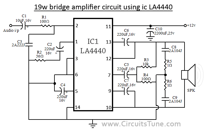
When the IC LA4440 is in Bridge mode in the circuit, its output power is 19w. In bridge mode use 4Ω-8Ω speaker. If you want stereo output(19w+19w) in bridge mode then use two copies of amplifier circuit of given below. Resistor R3&R4 is to adjust the voltage gain and for making input signal of inverting amplifier.

Bridge Amplifier Circuit using  IC LA4440
Fig-2: LA4440 Bridge Amplifier Circuit Diagram

Circuit description for both, stereo and bridge amplifier mode


C10 is filter capacitor used to reduce the ripple of supply voltage. Don’t decrease the value of capacitor C6&C7 less than 100uF, 10v, it may causes of the output at low frequencies goes lower. The pin-6 of LA4440 amplifier circuit  is audio input pin; it used in stereo amplifier mode but in bridge mode it is grounded. C8&C9 are polyester film capacitor used to preventing oscillation, and R1&R2 used for the same reason as filter resistor. Though the maximum supply voltage for both circuit of amplifier is 18V but we recommend to use a 12V,3A power supply. Use a good quality heat sink with LA4440.

I think here you see little comparison between stereo and bridge amplifier of LA4440. If you want to make this amplifier project, then I recommend you the bridge one. I think it is ideal for a beginner. And I love its wattage rather than Stereo mode. There is also a possibilities as I say, make two copies of circuit of bridge amplifier for stereo, it will give you 19w+19w of audio power output.
Continue Reading..

Thursday, December 26, 2013

This can also expand the brand mobile phone manufacturers

cell phone jammer can help the school prevent students against using the cell phone in the improper time.
Recycling of electronic products under the generally applicable "producer responsibility" principle, responsible for waste recycling mobile phones and other electronic products, primarily responsible for the use of the mobile phone manufacturer, that manufacturer should be used mobile phones and other electronic products recycling and utilization of play a major role. Major brand mobile phone manufacturers should set up a special cell phone recycling organization will be incorporated into the service of mobile phone recycling. Can be recycled to the cell phone repair and renovation of the old channels after the regular sale to economically underdeveloped areas, to expand sales of mobile phone market. This can also expand the brand mobile phone manufacturers, mobile phone manufacturers such behavior will be recognized by consumers. For businesses, reputation is an intangible asset. The most important thing is good publicity, so that users know that mobile phones and other electronic products recycling pathway. Can hold a number of recycling activities can enhance the users participation in environmental awareness. Innovation and recovery, so that people in the process of recycling used batteries to get a sense of psychological pleasure; paid recycling, so that people get the corresponding labor compensation; publicity and education so that people value their sense of identity recovery behavior. However, the low return rate for disposal of batteries, long cycle efficiency, it is difficult to attract investors, so it is difficult to form industrial scale, and produce benefits. In fact, used cell phone battery recycling industry is not profitable. Contains a large number of used cell phone batteries can be recycled such as heavy metals and acid substances, such as lead-acid battery recycling mainly recycling of lead-based waste, but also for the use of waste acid and plastic casing.  With the popularity of mobile phones, used cell phone batteries have become a special type of e-waste, the current cell phone batteries are Cd-Ni, MH-Ni and Li-ion three types of batteries, Cd-Ni battery is the main pollutants Ni, Cd and KOH, nickel-metal hydride battery is the main pollutants Cd, Cu and KOH, lithium-ion battery is the main pollutant Co, Mn and organic electrolytes. The resulting environmental pollution and waste of resources has become increasingly prominent. Used cell phone batteries on the environment and human health hazards mainly from the one containing the acid, alkali and heavy metals such as electrolyte solution. At present, China is mainly used mobile phone batteries with household waste in landfills, incineration, composting and other methods for processing, and waste batteries if the joint deal with the garbage man will be brought to the environment and great potential harm.
Continue Reading..

Pulse Charger for Reviving Tired Lead Acid Batteries

If you own a motorcycle, a motor home, a caravan, a lawn mover, a day cruiser or maybe a vintage car you must at some point had to write off a lead acid battery. When a battery is improperly charged or allowed to self-discharge as occurs during non-use, sulphate crystals build up on the batterys plates. The sulphate preventing the battery from being fully charged and therefore it is unable to deliver its full capacity. When trying to charge a battery in this state it only gets hot and looses water, the gravity of the electrolyte is not increasing to its normal “full charge” state. The only thing you do is killing the battery completely. If a battery has a resting voltage of at least 1.8 Volts/cell and no cells are shorted, desulphation of its plates can be done. This circuit is an add-on and part for a modification of a normal charger and it takes care of the sulphate problem.

Pulse Charger for Reviving Tired Lead Acid Batteries Circuit diagram:

Pulse Charger for Reviving Tired-Lead Acid Batteries-Circuit diagram

CAUTION:

Before you begin a project like this remember: mains voltage is dangerous so if you are not 100% sure of what you’re doing consult a friend who has the skills or, don’t do it at all !

The project: get hold of an old charger, big or small it’s your choice depending on the size of batteries you normally handle (bigger is better). There are some tricks to boost the performance if you need it. Start by ripping out everything except the transformer and the rectifier. Some older chargers are equipped with fin rectifiers, which have high voltage drop and must be replaced. Replace with a rugged bridge rectifier that can cope with the amperes. All wiring on secondary should be short and heavy wire. The rectifier should be bolted to the chassis to keep cool. If the charger have a high/low switch it’s a bonus, if not you can in some cases add a few turns of wire on the secondary winding. The circuit; a 14-stage ripple counter and oscillator IC 4060 produce a pulse, which is the heartbeat of the circuit. The pulse is feed to the 555 timer that deicide the length of the active output. With the switch you can select long or short pulse output. The output of the 555 timer triggers the zero-cross optoisolator triac driver MOC 3041 via a transistor. This gives the charger transformer a soft start via the triac and the snubber circuit. A small power supply is necessary for the circuit and consists of T1 a transformer 15V 0.1A secondary, a bridge rectifier, a regulator and two caps. Because this project include a charger that is (X) the outcome can differ in performance from one case to another. However this do not mean that your project doesn’t work, but the efficiency can vary. Some notes the snubbercap is a high voltage AC type (X) and the resistors on the mains side is at least 0.5W type. Use a triac that can take 400V+ and 10A+, I use BTA 25.600 but this is overkill in most cases. No PCB sorry!

How it works:

Well the short version. The object is to get the cell voltage high enough for the sulphate to dissolve without boiling or melting the battery. This is achieved by applying higher voltage for shorter periods and let the battery rest for a while. The pulses on short range is about 0.5s on / 3s off and the long pulse range is 1.4s on / 2s off. These times can vary depending on component tolerances. Start on long pulse and if you discover “boiling” (more than with normal charging) in the electrolyte switch to short puls. Don’t leave the process unattended, at least until you know how your specific version of this project turns out. I built ver.1 of this circuit some 10 years ago and have experimented with it but I’m sure someone can improve it further.

Good Luck! Ante
Ante135@hotmail.com

Continue Reading..

Tuesday, December 24, 2013

Cable Tester

This cable tester allows you to quickly check audio cables for broken wires. Because of the low power supply voltage, batteries can be used which makes the circuit portable, and therefore can be used on location.

Cable Tester Circuit diagram:

Simple Cable Tester-Circuit Diagram

The design is very simple and well organ-ised: using the rotary switch, you select which conductor in the cable to test. The corresponding LED will light up as indication of the selected conductor. This is also an indication that the power supply volt-age is present. If there is a break in the cable, or a loose connection, a second LED will light up, corresponding to the selected conductor. You can also see immediately if there is an internal short circuit when other than the corresponding LEDs light up as well.

You can also test adapter and splitter cables because of the presence of the different connectors.
Two standard AA- or AAA- batteries are sufficient for the power supply. It is recommended to use good, low-current type LEDs. It is also a good idea not to use the cheapest brand of connectors, otherwise there can be doubt as to the location of the fault. Is it the cable or the connector.

Source:   http://www.ecircuitslab.com/2012/06/simple-cable-tester.html
Continue Reading..

Monday, December 23, 2013

New Automatic Shutoff Battery Charger Circuit Diagram

This is a New Automatic Shutoff Battery Charger Circuit Diagram. This automatic shutoff battery charger circuit diagram Adjust by setting the 500 ohm resistor while attached to a fully charged battery.

New Automatic Shutoff Battery Charger Circuit Diagram

New Automatic Shutoff Battery Charger Circuit Diagram

Continue Reading..

Saturday, December 21, 2013

The security is installing cell phone jammer in the hall

The security is installing cell phone jammer in the hall
Store the device in cold areas, when the cell phone temperature, moisture can form inside cell phone circuit board caused by the destruction. A cell phone the other is not being used next to the program-controlled telecell phones: Avoid next to are using a program-controlled telecell phone using the GSM cell phone, GSM cell phone with the program-controlled telecell phone interference greatly, as well as the two sides could not hear. Note Save the cell phone and its components: Do not drop, knock, or shake the device, Rough handling can break internal circuit boards. Note that usually your cell phone and its parts, and accessories out of childrens reach, to prevent accidents caused by damage to the cell phone. You can buy a holster, usually to put a protective clothing. Never use harsh chemicals, cleaning solvents or strong detergents to clean the cell phone. Clear internal screen dust: to prepare a roll of sealing a wide paper tape, the single piece of adhesive tape attached to the machines internal display on the reverse shell inside the shell, attach a snapping compaction, remove tape paper, assembly machines.
To enter the Cell phone Wizard - File Manager - Enter the password (if not change your password is the default 123) - to find the encrypted file - Options - Encryption (more than one file is encrypted, the first tag, and then encryption). Cell phone Wizard can only encrypt files, and does not encrypt the folder, can see the encrypted file, Y-or Q-Manager, a can not be opened ... just go to the cell phone wizard decrypt file management, and point option selected decryption can. Encrypted using a cell phone lock. Starting a cell phone lock will open the file the program locks, there is no password to open this program, so as to achieve the purpose of the encrypted file.
A: officesuite can view and edit TXT file, is: Whether you TXT file in which folder to find the file open, direct calls officesuite. DOC document procedures, You can view and edit, save still saved in the original location. So that we can COPY from the computer text file into our cell phone spare. (Note: the installed officesuite was click on the TXT file with "Notepad" program to open the cell phone, stored in a directory on the Notepad, and now can not be used Notepad to open the, unless you have a text file in the directory on the Notepad) to question 26, why can not find my 100 access to audio-visual cell phones UMD and TXT e-book?As follows: right click on the program, select Properties, select the compatibility 2000 compatibility mode.
Continue Reading..

Friday, December 20, 2013

100W Inverter Schematic

Here is a 100 Watt inverter circuit using minimum number of components. I think it is quite difficult to make a decent one like this with further less components.Here we use CD 4047 IC from Texas Instruments for generating the 100 Hz pulses and four 2N3055 transistors for driving the load. The IC1 Cd4047 wired as an astable multivibrator produces two 180 degree out of phase 100 Hz pulse trains.

These pulse trains are preamplified by the two TIP122 transistors.The out puts of the TIP 122 transistors are amplified by four 2N3055 transistors (two transistors for each half cycle) to drive the inverter transformer.The 220V AC will be available at the secondary of the transformer. Nothing complex just the elementary inverter principle and the circuit works great for small loads like a few bulbs or fans.If you need just a low cost inverter in the region of 100 W, then this is the best.

 100 Watt Inverter Circuit diagram:

100watt  inverter circuit schematic diagram
Parts:
P1 = 250K
R1 = 4.7K
R2 = 4.7K
R3 = 0.1R-5W
R4 = 0.1R-5W
R5 = 0.1R-5W
R6 = 0.1R-5W
C1 = 0.022uF
C2 = 220uF-25V
D1 = BY127
D2 = 9.1V Zener
Q1 = TIP122
Q2 = TIP122
Q3 = 2N3055
Q4 = 2N3055
Q5 = 2N3055
Q6 = 2N3055
F1 = 10A Fuse
IC1 = CD4047
T1 = 12-0-12V
Transformr Connected in Reverse
Notes:
  • A 12 V car battery can be used as the 12V source.
  • Use the POT R1 to set the output frequency to50Hz.
  • For the transformer get a 12-0-12 V , 10A step down transformer.But here the 12-
  • 0-12 V winding will be the primary and 220V winding will be the secondary.
  • If you could not get a 10A rated transformer , don’t worry a 5A one will be just
  • enough. But the allowed out put power will be reduced to 60W.
  • Use a 10 A fuse in series with the battery as shown in circuit.
  • Mount the IC on a IC holder.
  • Remember,this circuit is nothing when compared to advanced PWM
  • inverters.This is a low cost circuit meant for low scale applications.
Design tips:
  1. The maximum allowed output power of an inverter depends on two factors.The
  2. maximum current rating of the transformer primary and the current rating of the driving
  3. transistors.
  4. For example ,to get a 100 Watt output using 12 V car battery the primary current will be
  5. ~8A ,(100/12) because P=VxI.So the primary of transformer must be rated above 8A.
  6. Also here ,each final driver transistors must be rated above 4A. Here two will be
  7. conducting parallel in each half cycle, so I=8/2 = 4A .
  8. These are only rough calculations and enough for this circuit.
Source :   http://www.ecircuitslab.com/2011/06/100w-inverter-circuit-diagram-schematic.html
Continue Reading..

Thursday, December 19, 2013

Multi Color LED

How many different conditions do you reckon may be signalled with just one LED? Two, maybe three? Using this simple circuit, a lot more!


Admittedly, a two-colour LED is used here. Such a device consists of two light-emitting chips, usually red and green, encapsulated in the same case. It has three pins: two for the anodes, and one for the common cathode. In this way, each diode can be activated separately. Various mixed colours may be obtained by varying the current through the two diodes. At least four discrete colours are then easily perceived: pure red, pure green, orange (IR ≈ 2IG) and yellow (IG ≈ 2IR).

In the present circuit, the LED elements are driven by CMOS three-state buffers type 4503, which, unlike most CMOS ICs from the 4000 series, are capable of supplying up to 10 mA of output current. The LED cur-rents are limited by resistors R1 through R6, whose values invite experiments with brightness and colours according to your own taste.


Simple Multi-Color LED Circuit diagram:

Simple Multi-Color LED-Circuit Diagram


The circuit was originally developed to indicate the state of three inputs, a, b, and c (non-binary, i. e., only one of these is at 1 at any time), with the con-figuration (a=b=c=0) representing the fourth state. The latter is decoded by NAND gate IC1. An additional effect is produced by gates IC1a and IC1b, which are connected up into an oscillator circuit producing approximately two pulses per second. These pulses are used to control the common-enable input, DA (pin 1) of the 4503, so as to produce a flickering effect. The oscillator is controlled by means of inputs ‘d’ and ‘e’. Pulling both of these logic high disables the oscillator and the LED driver. With e=0 and d=1 the outputs of the 4503 are switched to three-state, and the circuit is in power-down standby mode.

Although designed for a 12-V supply voltage, the circuit will happily work at any supply volt-age between 5 V and 16 V. Non-used inputs of CMOS ICs must, of course, be tied to ground via 10-100 kW resistors.

Source: http://www.ecircuitslab.com/2012/06/simple-multi-color-led.html
Continue Reading..

Wednesday, December 18, 2013

Telephone line Based Audio Muting and Light On

Very often when enjoying music or watching TV at high audio level, we may not be able to hear a telephone ring and thus miss an important incoming phone call. To overcome this situation, the circuit presented here can be used. The circuit would automatically light a bulb on arrival of a telephone ring and simultaneously mute the music system/TV audio for the duration the telephone handset is off-hook. Lighting of the bulb would not only indicate an incoming call but also help in locating the telephone during darkness.

Telephone line Based Audio Muting and Light-On Circuit Diagram

Telephone line Based Audio Muting and Light-On Circuit Diagram
On arrival of a ring, or when the handset is off-hook, the inbuilt transistor of IC1 (opto-coupler) conducts and capacitor C1 gets charged and, in turn, transistor T1 gets forward biased. As a result, transistor T1 conducts, causing energisation of relays RL1, RL2, and RL3. Diode D1 connected in antiparallel to inbuilt diode of IC1, in shunt with resistor R1, provides an easy path for AC current and helps in limiting the voltage across inbuilt diode to a safe value during the ringing. (The RMS value of ring voltage lies between 70 and 90 volts RMS.) Capacitor C1 maintains necessary voltage for continuously forward biasing  transistor T1 so that the relays are not energised during the negative half cycles and off-period of ring signal. Once the handset is picked up, the relays will still remain energised because of low impedance DC path available (via cradle switch and handset) for the in-built diode of IC1.

After completion of call when handset is placed back on its cradle, the low-impedance path through handset is no more available and thus relays RL1 through RL3 are deactivated. As shown in the figure, the energised relay RL1 switches on the light, while energisation of relay RL2 causes the path of TV speaker lead to be opened. (For dual-speaker TV, replace relay RL2 with a DPDT relay of 6V, 200 ohm.) Similarly, energisation of DPDT relay RL3 opens the leads going to the speakers and thus mutes both audio speakers. Use ‘NC’ contacts of relay RL3 in series with speakers of music system and ‘NC’ contacts of RL2 in series with TV speaker. Use  ‘NO’ con-tact of relay RL1 in series with a bulb to get the visual indication.

Source: http://www.ecircuitslab.com/2011/12/telephone-line-based-audio-muting-and.html


Continue Reading..

Tuesday, December 17, 2013

Video Isolator

These days many more audio-visual devices in the home are connected together. This is especially the case with the TV, which may be connected to a DVD player, a hard disk recorder, a surround-sound receiver and often a PC as well. This often creates a problem when earth loops are created in the shielding of the video cables, which may cause hum and other interference. The surround-sound receiver contains a tuner that takes its signal from a central aerial distribution system. The TV is also connected to this and it’s highly likely that the PC has a TV-card, which again is connected to the same system. On top of this, there are many analogue connections between these devices, such as audio cables. The usual result of this is that there will be a hum in the audio installation, but in some cases you may also see interference on the TV screen.

The ground loop problem can be overcome by galvanically isolating the video connections, for example at the aerial inputs of the surround-sound receiver and the TV. Special adaptors or filters are sold for this purpose, known as video ground loop isolators. Good news: such a filter can also be easily made at home by yourself. There are two ways in which you can create galvanic isolation in a TV cable. The first is to use an isolating transformer with two separate windings. The other is to use two coupling capacitors in series with the cable. The latter method is easily the simplest to implement and generally works well enough in practice. The simplest way to produce such a ‘filter’ is as an in-line adapter, so you can just plug it onto either end of a TV aerial cable.

Video Isolator Circuit diagram:


The only requirements are a male and female coax plug and two capacitors. The latter have to be suitable for high-frequency applications, such as ceramic or MKT types. It is furthermore advisable to choose types rated for high voltages (400 V), since the voltages across these capacitors can be higher than you might expect (A PC that isn’t connected to the mains Earth can have a voltage as high as 115 V (but at a very low, safe current), caused by the filter capacitors in its power supply. These capacitors don’t need to be high value ones, since they only have to pass through frequencies above about 50 MHz. Values of 1 nF or 2.2 nF are therefore sufficient. To make the isolator you should connect one capacitor between the two earth connections of the coax plugs and the other between the two signal connections.

The mechanical construction has to be sturdy enough such that the connections to the capacitors won’t break whenever the inline adapter is removed forcibly. A good way to do this is to make a cover from a piece of PVC piping for the central part. Wrap aluminium foil round the outside and connect it to one of the plugs, so that the internal parts are properly shielded from external interference. Make sure that the aluminium foil doesn’t make contact with the other plug, otherwise you lose the isolation. The majority of earth loops will disappear when you connect these filters to all used outputs of the central aerial distribution system where the signal enters the house.
Harry Baggen
 
Copyright : Elektor Electronics 2008

Source:http://www.ecircuitslab.com/2011/07/video-isolator-circuit-diagram.html
Continue Reading..

Monday, December 16, 2013

Switching inverter for 12v systems circuit diagram

This PWM control circuit provides the control pulse to the DMOS Power Switch in the flyback circuit. The output of the PWM is a pulse whose width is proportional to the input control voltage and whose repetition rate is determined by an external clock signal. 

To provide the control input to the PWM and to prevent the output voltage from soaring or sagging as the load changes the error amplifier and reference voltage complete the design. They act as the feedback loop in this control circuit much like that of a servo control system.


Switching inverter for 12v systems circuit diagram

Switching inverter for 12v systems circuit diagram

Continue Reading..

Thursday, October 10, 2013

Liquid Crystal Display LCD Tester

Liquid-crystal displays come in all sorts and sizes, and this applies also to their pinouts. In fact, many of these displays cannot be used properly without the manufacturers’ documentation. But, of course, this can never be found when it is needed, and a small tester to unravel the terminals may, therefore, be found very handy. A liquid-crystal display consists of two thin sheets of glass, the facing surfaces of which have been given thin conducting tracks. When the glass is looked through at right or near-right angles, these tracks cannot be seen. At certain viewing angles, they become visible, however.

The space between the sheets of glass is filled with a liquid that, stimulated by an electric voltage, alters the polarization of the incident light. In this way, segments may appear light or dark and give rise to the display of lines or shapes. A segment may be tested by applying an alternating voltage of a few volts across it. Note that the application of a direct voltage will damage the display irreversibly: the resulting current will remove the tracks. The alternating voltage should contain not even a tiny direct voltage component. An alternating current also removes part of the tracks when the current flows in one direction, but restores it when the current flows in the opposite direction.

Liquid-Crystal Display (LCD) Tester Circuit DiagramThe tester described here consists of a square-wave generator that produces an absolutely symmetrical alternating voltage without any d.c. component. Most logic oscillators are incapable of producing a squarewave signal: they generate rectangular waveforms whose duty cycle hovers around the 50%. The 4047 used in the tester has a binary scaler at its output that guarantees symmetry. The oscillator frequency is about 1 kHz. It may be powered from a 3–9 V source. Normally, this will be a battery, but a variable power supply has advantages. It shows at which voltage the display works satisfactorily and also that there is a clear relationship between the level of the voltage and the angle at which the display is clearly legible.

The tester draws a current not exceeding 1 mA. The test voltage must at all times be connected between the common terminal, that is, the back plane, and one of the segments. If it is not known which of the terminals is the back plane, connect one probe of the tester to a segment and the other successively to all the other terminals until the segment becomes visible. Note, however, that there are LCDs with more than one back plane. Therefore, if a segment does not become visible, investigate whether the display has a second back plane terminal.
Continue Reading..

Wednesday, October 9, 2013

Mains Slave Switcher II

As a guide, a one-inch reed switch with 40 turns reliably switched on with the current flowing through a 150-watt lamp (approx. 625 mA) but larger reeds may require more turns. If the master appliance draws less current (which is unlikely with power tools) more turns will be required. The reed switch is used to switch on transistor T1 which in turn switches the relay RE1 and powers the slave appliance. Since reed switches have a low mechanical inertia, they have little difficulty in following the fluctuations of the magnetic field due to the alternating current in the coil and this means that they will switch on and off at 100 Hz.
Circuit diagram:
mains-slave-switcher-circuit-diagram2
C3 is therefore fitted to slow down the transistor response and keep the relay energised during the mains zero crossings when the current drawn by the appliance falls to zero and the reed switch opens. C1 drops the mains voltage to about 15 V (determined by zener diode D1) and this is rectified and smoothed by D2 and C2 to provide a d.c. supply for the circuit. The relay contacts should be rated to switch the intended appliance (vacuum cleaner) and the coil should have a minimum coil resistance of 400 R as the simple d.c. supply can only provide a limited current. C1 drops virtually the full mains voltage and should therefore be a n X2-class component with a voltage rating of at least 250V a.c.
Warning:
The circuit is by its nature connected directly to the mains supply. Great care should therefore be taken in its construction and the circuit should be enclosed in a plastic or earthed metal box with mains sockets fitted for the master and slave appliances.
Author: Elektor - Copyright: Elektor Electronics Magazine
Continue Reading..

Tuesday, October 8, 2013

Build A Synchronous Clock

The quartz clocks which have dominated time-keeping for the past 20 years or so have one problem: their errors, although slight, are cumulative. After running for several months the errors can be significant. Sometimes you can correct these if you can slightly tweak the crystal frequency but otherwise you are forced to reset the clock at regular intervals. By contrast, mains-powered synchronous clocks are kept accurate by the 50Hz mains distribution system and they are very reliable, except of course, when a blackout occurs. This circuit converts a quartz clock to synchronous mains operation, so that you can have at least one clock in your home which shows the time. First, you need to obtain a quartz clock movement and disassemble it down to the PC board. For instructions on how to do this, see the article on a "Fast Clock For Railway Modellers" in the December 1996 issue of SILICON CHIP. Then isolate the two wires to the clock coil and solder two light duty insulated hookup wires to them (eg, two strands of rainbow cable). Drill a small hole in the clock case and pass the wires through them. Then reassemble the clock case.

Circuit diagram:

building_a_synchronous_clock circuit

A Synchronous Clock Circuit Diagram

To test the movement, touch the wires to the terminals of an AA cell, then reverse the wires and touch the cell terminals again. The clock second hand should advance on each connection. The circuit is driven by a low voltage AC plug pack. Its AC output is fed to two bridge rectifiers: BR1 provides the DC supply while BR2 provides positive-going pulses at 100Hz to IC1a, a 4093 NAND Schmitt trigger. IC1a squares up the 100Hz pulses and feeds them to the clock input of the cascaded 4017 decade counters. The output at pin 12 of IC3 is 1Hz. This is fed to IC4, a 4013 D-type flipflop, which is connected so that its two outputs at pins 12 & 13 each go positive for one second at a time. As these pulses are too long to drive the clock movement directly, the outputs are each fed to 4093 NAND gates IC1b & IC1c where they are gated with the pin 3 signal to IC4. This results in short pulses from pins 3 & 10 of IC1 which drives the clock via limiting resistor R1. The value of R1 should be selected on test, allowing just enough current to reliably drive the clock movement.

Author: A. J. Lowe - Copyright: Silicon Chip

Continue Reading..

Monday, October 7, 2013

Antenna Tuning Unit ATU For 27 MHz CB Radios

This antenna tuning unit (ATU) enables half-wavelength or longer wire antennas to be matched to the 50-? antenna input of 27-MHz Citizens’ Band (CB) rigs. The ATU is useful in those cases where a wire antenna is less obtrusive than a roof-mounted ‘vertical’ or ground-plane. It is also great for ‘improvised’ antennas used by active CB users on camping sites and the like because it allows a length of wire to be used as a fairly effective antenna hung between, say, a tree branch at one side and a tent post, at the other. Obviously, the wire ends then have to be isolated using, for example, short lengths of nylon wire. It is even possible to use the ATU to tune a length of barbed wire to 27 MHz. The coil in the circuit consists of 11 turns of silver-plated copper wire with a diameter of about 1 mm (SWG20).

The internal diameter of the coil is 15 mm, and it is stretched to a length of about 4 cm. The tap for the antenna cable to the CB radio is made at about 2 turns from the cold (ground) side. Two trimmer capacitors are available for tuning the ATU. The smaller one, C1, for fine tuning, and the larger one, C2, for coarse tuning. The trimmers are adjusted with the aid of an in-line SWR (standing-wave ratio) meter which most CB enthusiasts will have, or should be able to obtain on loan. Select channel 20 on the CB rig and set C1 and C3 to mid-travel. Press the PTT button and adjust C2 for the best (that is, lowest) SWR reading. Next, alternately adjust C3 and C2 until you get as close as possible to a 1:1 SWR reading.

Antenna Tuning Unit (ATU) For 27-MHz CB RadiosC1 may then be tweaked for an even better value. No need to re-adjust the ATU until another antenna is used. In case the length of the wire antenna is exactly 5.5 metres, then C3 is set to maximum capacitance. Although the ATU is designed for half-wavelength or longer antennas, it may also be used for physically shorter antennas. For example, if antenna has a physical length of only 3 metres, then the remaining 2.5 metres has to be wound on a length of PVC tubing. This creates a so-called BLC (base-loaded coil) electrically shortened antenna. In practice, the added coil can be made somewhat shorter than the theoretical value, so the actual length is best determined by trial and error. Finally, the ATU has to be built in an all-metal case to prevent unwanted radiation. The trimmers are than accessed through small holes. The connection to the CB radio is best made using an SO239 (‘UHF’) or BNC style socket on the ATU box and a short 50-W coax cable with matching plugs.
Continue Reading..

Sunday, October 6, 2013

Speach Amplifier Circuit Diagram

This circuit is intended to be placed in the same box containing the loudspeaker, forming a compact microphone amplifier primarily intended for speech reinforcement. A device of this kind is particularly suited to teachers, lecturers, tourists guides, hostesses and anyone speaking in crowded, noisy environment.

The circuits heart is formed by the TDA7052 Audio power amplifier IC, delivering a maximum output of 1.2W @ 6V supply. An external microphone must be plugged into J1, its signal being amplified by Q1 and fed to IC1. R1 acts as a volume control and C3 tailors the upper audio frequency band, mainly to reduce the microphone possibility of picking-up the loudspeaker output, causing a very undesirable and loud "howl", i.e. the well known Larsen effect. Therefore, C3 value can be varied in the 4n7 - 22nF range to ensure the best compromise from speech tone quality and minimum Larsen effect occurrence. Dynamic or electrets microphone is warmly recommended. It has a useful feature that can be used to momentarily mute the microphone by connecting SW1 shown in diagram.

Circuit Diagram:

Speech Amplifier Circuit Diaram Speach Amplifier Circuit Diagram

Parts Description
R1 22K
R2 1M
R3 15K
R4 470R
R5 47K
R6 4.7K
C1 100nF-63V
C2 100nF-63V
C3 100nF-63V
C4 10nF-63V
C5 220uF-25V
C6 10uF-25V
Q1 BC547
IC1 TDA7052 B1
J1 Mono Jack Socket
B1 6V Battery
SW1 SPST Slider Switch
SW2 SPST Toggle Switch

Notes:

  • Please note that hands-free, uni-directional headset or ear clip microphone types are very well suited for this device, as also are Clip-on Lavaliere or Lapel microphones.
  • If a small electrets capsule is used for the microphone, R5, R6 and C6 must be added to the circuit to provide power supply.
  • Choose a loudspeaker as large as possible, in order to increase circuit performance.
  • You can use also two 4 Ohm loudspeakers wired in series or two 8 Ohm types wired in parallel in order to obtain better results.
  • The box containing the amplifier and loudspeaker(s) can be fitted out with a belt and carried like a shoulder-bag or, if you build a smaller unit, it can be used as a Pick & Go Belt Clip Speaker.

Source : www.redcircuits.com

Continue Reading..

Saturday, October 5, 2013

Fuse Box BMW 318i 1995 Diagram

Fuse Box BMW 318i 1995 Diagram - Here are new post for Fuse Box BMW 318i 1995 Diagram.

Fuse Box BMW 318i 1995 Diagram


Fuse Box BMW 318i 1995 Diagram

Fuse Panel Layout Diagram Parts: hazard flasher relay, low beam light relay, high beam light relay, blower relay, front fog light relay, horn relay.
Continue Reading..

Friday, October 4, 2013

4 20mA Current Loop Tester

This design will interest technicians who work on pneumatically operated valves and other 4-20mA current loop controlled devices. Although 4-20mA signal injector/calibrators are available, this one is both cheap to build and easy to operate. When first powered up, the circuit sinks 4mA of current. If switch S1 is pressed, the current level slowly ramps up to 20mA, pauses and then ramps back to 4mA. This cycle will continue unless the switch is pressed again, whereby the output will lock to its current level. A further push of the switch resumes the prior cyclic operation. Output2 from the micro (IC1) is programmed to generate a pulse-width modulated (PWM) signal to drive the current sink transistor (Q1).

4-20mA Current Loop Tester circuit schematic
The digital PWM signal is converted to an analog voltage using a low-pass filter formed by the 1kω series resistor and a 4.7μF tantalum capacitor. By varying the PWM duty cycle and therefore the DC signal level out of the filter, the program can indirectly vary the current flow through the transistor. A 100 resistor in series with the emitter of Q1 converts the loop current to a small voltage, which is fed into the micro on input1. The program uses this feedback signal to zero in on the desired current level with the aid of the micros analog-to-digital converter. Details of this can be seen in the accompanying program listing.

If the PICAXE senses an open circuit, it shuts down the output and goes into an alarm state, to alert the operator and protect the circuit under test. The switch can be pressed to reset operations to the start once the open circuit has been rectified. The LED flashes a code for various milestones, as follows: one flash at 4m and one flash to confirm a switch press two flashes at 12m when ramping up (for the first 5 cycles); three flashes at 20m and continued fast flash sequence for open-circuit alarm. For portable use, the circuit can be powered from two 9V batteries, whereas for bench testing, a 12V DC plugpack will suffice.
Continue Reading..

Thursday, October 3, 2013

LED Volt Meter Circuit

Here is a Simple LED Volt meter to Monitor the charge level in Lead Acid Battery or Tubular battery. The terminal voltage of the battery is indicated through a four level LED indicators. The nominal terminal voltage of a Lead Acid battery is 13.8 volts and that of a Tubular battery is 14.8 volts when fully charged. The LED voltmeter uses four Zener diodes to light the LEDs at the precise breakdown voltage of the Zener diodes. Usually the Zener diode requires 1.6 volts in excess than its prescribed value to reach the breakdown threshold level. When the battery holds 13.6 volts or more, all the Zener breakdown and all LEDs light up. When the battery is discharged below 10.6 volts, all the LEDs remain dark. So depending on the terminal voltage of the battery, LEDs light up one by one or turns off.

Circuit diagram:

LED-Volt-Meter-circuit-diagram12 LED Volt Meter Circuit Diagram

Author: D. Mohan Kumar Copyright: electroschematics.com

Continue Reading..

Wednesday, October 2, 2013

Adjustable Zener Diode

A Zener diode is the simplest known type of voltage limiter (Figure 1) As soon as the voltage exceeds the rated voltage of the Zener diode, a current can flow through the diode to limit the voltage. This is exactly the right answer for many protection circuit applications. However, if it is necessary to limit a signal to a certain voltage in a control circuit, Zener diodes do not provide an adequate solution. They are only available with fixed values, which are also subject to a tolerance range. What we are looking for is thus an ‘adjustable’ Zener diode. Such a component would be useful in a heating controller with a preheat temperature limiting, for example, or in a battery charger to provide current limiting. The answer to our quest is shown in Figure 2. Assume for example that the output voltage must not exceed 6.5 V. The control voltage on the non-inverting input is thus set to 6.5 V.

Adjustable Zener Diode circuit schematic

Now assume that 4.2V is present at the input. The result is that the maximum positive voltage is present at the opamp output, but the diode prevents this from having any effect on the signal. However, if the voltage rises above 6.5V, the output of the opamp goes negative and pulls the voltage back down to 6.5 V. The current is limited by R3. Another example is a situation in which exactly the opposite is required. In this case, the voltage must not drop below a certain value. This can be easily achieved by reversing the polarity of the diode. Another option is a voltage that is only allowed to vary within a certain voltage window. It must not rise above a certain value, but it also must not drop below another specific value. In the circuit shown in Figure 3, the left-hand opamp provides the upper limit and the right-hand opamp provides the lower limit. Each opamp is wired as a voltage follower.
Continue Reading..

Tuesday, October 1, 2013

Model Railway Short Circuit Beeper

Short circuits in the tracks, points or wiring are almost inevitable when building or operating a model railway. Although transformers for model systems must be protected against short circuits by built-in bimetallic switches, the response time of such switches is so long that is not possible to immediately localise a short that occurs while the trains are running, for example. Furthermore, bimetallic protection switches do not always work properly when the voltage applied to the track circuit is relatively low. The rapid-acting acoustic short-circuit detector described here eliminates these problems. However, it requires its own power source, which is implemented here in the form of a GoldCap storage capacitor with a capacity of 0.1 to 1 F. A commonly available reed switch (filled with an inert gas) is used for the current sensor, but in this case it is actuated by a solenoid instead of a permanent magnet.

An adequate coil is provided by several turns of 0.8–1 mm enamelled copper wire wound around a drill bit or yarn spool and then slipped over the glass tube of the reed switch. This technique generates only a negligible voltage drop. The actuation sensitivity of the switch (expressed in ampère-turns or A-t)) determines the number of turns required for the coil. For instance, if you select a type rated at 20–40 A-t and assume a maximum allowable operating current of 6 A, seven turns (40 ÷ 6 = 6.67) will be sufficient. As a rule, the optimum number of windings must be determined empirically, due to a lack of specification data. As you can see from the circuit diagram, the short-circuit detector is equally suitable for AC and DC railways. With Märklin transformers (HO and I), the track and lighting circuits can be sensed together, since both circuits are powered from a single secondary winding.

Model Railway Short-Circuit Beeper circuit schematic

Coil L1 is located in the common ground lead (‘O’ terminal), so the piezoelectric buzzer will sound if a short circuit is present in either of the two circuits. The (positive) trigger voltage is taken from the lighting circuit (L) via D1 and series resistor R1. Even though the current flowing through winding L1 is an AC or pulsating DC current, which causes the contact reeds to vibrate in synchronisation with the mains frequency, the buzzer will be activated because a brief positive pulse is all that is required to trigger thyristor Th1. The thyristor takes its anode voltage from the GoldCap storage capacitor (C2), which is charged via C2 and R2.

The alarm can be manually switched off using switch S1, since although the thyristor will return to the blocking state after C2 has been discharged if a short circuit is present the lighting circuit, this will not happen if there is a short circuit in the track circuit. C1 eliminates any noise pulses that may be generated. As a continuous tone does not attract as much attention as an intermittent beep, an intermittent piezoelectric generator is preferable. As almost no current flows during the intervals between beeps and the hold current through the thyristor must be kept above 3 mA, a resistor with a value of 1.5–1.8 kΩ is connected in parallel with the buzzer. This may also be necessary with certain types of continuous-tone buzzers if the operating current is less than 3 mA. The Zener diode must limit the operating voltage to 5.1 V, since the rated voltage of the GoldCap capacitor is 5.5V.
Continue Reading..

Monday, September 30, 2013

Petrol Gas Switch For A Pajero

My current vehicle, a Pajero, was modified for dual fuel - ie, petrol and gas. However, its necessary to run the vehicle on petrol at regular intervals to stop the injectors from clogging up. This simple circuit allows the vehicle to be started using petrol and then automatically switches it to gas when the speed exceeds 45km/h and the brake pedal is pressed. Alternatively, the vehicle may be run on petrol simply by switching the existing petrol/gas switch to petrol.

You can also start the vehicle on gas by pressing the brake pedal while starting the vehicle. The circuit is based on an LM324 dual op amp, with both op amps wired as comparators. It works like this: IC1a buffers the signal from the vehicles speed sensor and drives an output filter network (D1, a 560kO resistor and a 10µF capacitor) to produce a DC voltage thats proportional to the vehicles speed.

Circuit diagram:

petrol-gas-switch-for-a-pajero

Petrol Gas Switch For A Pajero Circuit diagram

This voltage is then applied to pin 5 of IC1b and compared with the voltage set by trimpot VR1. When pin 7 of IC1b goes high, transistor Q1 turns on. This also turns on transistor Q2 when the brake pedal is pressed (pressing the brake pedal applies +12V from the brake light circuit to Q2s emitter). And when Q2 turns on, relay 1 turns on and its contacts switch to the gas position. Trimpot VR1 must be adjusted so that IC1bs pin 7 output switches high when the desired trigger speed is reached (ie, 45km/h). In effect, the speed signal is ANDed with the brake light signal to turn on the relay. The vehicle has been running this circuit for several years now and is still running well, with no further injector cleans required.

Author: J. Malnar - Copyright: Silicon Chip Electronics

Continue Reading..

Sunday, September 29, 2013

Neon Flasher Runs From 3V Supply

A neon indicator typically requires at least 70V to fire it and normally would not be contemplated in a battery circuit. However, this little switchmode circuit from the Linear Technology website (www.linear-tech.com) steps up the 3V battery supply to around 95V or so, to drive a neon with ease. The circuit has two parts: IC1 operating as step-up converter at around 75kHz and a diode pump, consisting of three 1N4148 diodes and associated .022µF capacitors. The 3.3MO resistor and the 0.68µF capacitor set the flashing rate to about once every two seconds. The average DC level from the diode pump is set to about 95V by the 100MO feedback resistor to pin 8. The circuit could also use an LT1111 (RS Components Cat 217-0448) which would run at about 20kHz so L1 could be reduced to 100mH and use a powdered iron toroid core from Neosid or Jaycar.

neon flasher circuit schematic
Continue Reading..

Saturday, September 28, 2013

Modular Phono Preamplifier


High Quality Moving Magnet Pick-up module
Two-stage Series/Shunt feedback RIAA equalization


Any electronics amateur still in possess of a collection of vinyl recordings and aiming at a high quality reproduction should build this preamp and add it to the Modular Preamplifier chain. This circuit features a very high input overload capability, very low distortion and accurate reproduction of the RIAA equalization curve, thanks to a two-stage op-amp circuitry in which the RIAA equalization network was split in two halves: an input stage (IC1A) wired in a series feedback configuration, implementing the bass-boost part of the RIAA equalization curve and a second stage, implementing the treble-cut part of the curve by means of a second op-amp (IC2A) wired in the shunt feedback configuration.

Modular Phono Preamplifier circuit diagramParts:

R1_____________270R 1/4W Resistor
R2_____________100K 1/4W Resistor
R3_______________2K2 1/4W Resistor
R4______________39K 1/4W Resistor
R5_______________3K9 1/4W Resistor
R6_____________390K 1/4W Resistor
R7______________33K 1/4W Resistor
R8______________75K 1/4W Resistor (or two 150K resistors wired in parallel)
R9_____________560R 1/4W Resistor
C1_____________220pF 63V Polystyrene or Ceramic Capacitor
C2_______________1µF 63V Polyester Capacitor
C3______________47µF 25V Electrolytic Capacitor
C4______________10nF 63V Polyester Capacitor 5% tolerance or better
C5_______________1nF 63V Polyester Capacitor 5% tolerance or better
C6,C9__________100nF 63V Polyester Capacitors
C7,C10__________22µF 25V Electrolytic Capacitors
C8,C11________2200µF 25V Electrolytic Capacitors
IC1___________LM833 or NE5532 Low noise Dual Op-amp
IC2___________TL072 Dual BIFET Op-Amp
IC3___________78L15 15V 100mA Positive Regulator IC
IC4___________79L15 15V 100mA Negative Regulator IC
D1,D2________1N4002 200V 1A Diodes
J1,J2___________RCA audio input sockets
J3______________Mini DC Power Socket

This module comprises also an independent dual rail power supply identical to that described in the Modular Preamplifier Control Center. As with the other modules of this series, each electronic board can be fitted into a standard enclosure: Hammond extruded aluminum cases are well suited to host the boards of this preamp. In particular, the cases sized 16 x 10.3 x 5.3 cm or 22 x 10.3 x 5.3 cm have a very good look when stacked. See below an example of the possible arrangement of the rear panel of this module.

Notes:
  • The circuit diagram shows the Left channel only and the power supply
  • Some parts are in common to both channels and must not be doubled. These parts are: IC3, IC4, C6, C7, C8, C9, C10, C11, D1, D2 and J3.
  • IC1 and IC2 are dual Op-Amps, therefore the second half of these devices will be used for the Right channel
  • This module requires an external 15 - 18V ac (50mA minimum) Power Supply Adaptor.
Technical data:

Sensitivity @ 1KHz: 4.3mV RMS input for 200mV RMS output
Max. input voltage @ 100Hz: 53mV RMS
Max. input voltage @ 1KHz: 212mV RMS
Max. input voltage @ 10KHz: 477mV RMS
Frequency response @ 200mV RMS output: flat from 30Hz to 23KHz; -0.5dB @ 20Hz
Total harmonic distortion @ 1KHz and up to 8.8V RMS output: 0.0028%
Total harmonic distortion @10KHz and up to 4.4V RMS output: 0.008%
Continue Reading..

Friday, September 27, 2013

Battery Replacement Power Supply

Your childs battery toy has failed and you have to fix it. Once you have managed to get it apart, the battery compartment is not likely to be connected to the works or the batteries might have gone flat anyway. The solution is this switchable supply which is designed to replace from one to six dry cells. It is not intended to replace the batteries on a permanent basis, as in most cases this is not practical. The heart of the supply is an LM317T adjustable 3-terminal regulator and six trimpots selected by switch S1b. The other pole of the switch, S1a, is used to select taps on the transformer secondary, to minimize power dissipation in the LM317T. The table shows the trimpot settings for the six voltage outputs. Diode D1 and the 10µF capacitor and the LED provide power indication. This has the advantage of constant brightness which would not be obtained if the LED was run from the unregulated switchable DC.

Battery replacement power supply circuit schematic
Continue Reading..

Thursday, September 26, 2013

Simple 6 Input Alarm

This simple alarm circuit was designed for use in a combined garage and rumpus room. It can be assembled on Veroboard and uses just one IC plus a handful of cheap components. The circuit is based on a straightforward 555 timer circuit (IC1). This is wired as a monostable and sets the siren period which is adjustable up to about three minutes using potentiometer VR1. In operation, IC1s pin 2 input monitors the detector circuit for negative-going signals. When a switch is closed, a brief negative-going pulse is applied to pin 2 via a 10µF capacitor and its corresponding series diode (D2-D7). This triggers IC1 which switches its pin 3 output high and switches off relay RLY1 (ie, RLY1 is normally on).

Simple 6-input alarm circuit schematic

As a result, the piezo siren sounds for the duration of the monostable period. In addition, relay RLY2 is turned on via diode D9 and latches on via D10. This means that the strobe light (which is wired to the normally open contact) will continue to flash until the alarm is switched off (via the keyswitch). At the end of the monostable period, RLY1 turns off and this turns off the piezo siren. The circuit can then be retriggered by any further trigger inputs from the switches. A variety of detectors with normally open contacts can be used for the switches, including reed switches, pressure mats, IR detectors and glass breakage detectors. All switches must be open before the alarm is switched on.
Continue Reading..

Wednesday, September 25, 2013

Stepper Motor Generator

Any stepper motor can be used as a generator. In contrast to other generators, a stepper motor produces a large induced voltage even at low rotational speeds. The type used here, with a DC resistance of 2×60 Ω per winding, can generate more than 20 V when turned by hand, without any gearing. The circuit diagram for a ‘hand-cranked torch’ shows how you can use a stepper motor as a generator. A supplementary circuit stores the energy. Two bridge rectifiers, each made up of four 1N4148 diodes, charge the 4700µF capacitor. The super-bright (white) LED is driven either via a 390-Ω resistor (Power Light), or via 22 kΩ in series with 390 Ω. In the latter case, the LED is not as bright, but it stays on longer.

Stepper Motor Generator circuit diagramYou must restrain yourself when cranking the dynamo, since in the ‘bright’ setting it is possible to exceed the rated LED current of 20mA, while in the ‘long’ setting it is possible to exceed the rated capacitor voltage of 25 V. If necessary, adjust the value of the LED series resistor. The lamp is bright enough for reading in complete darkness. The stepper motor generator is thus ideal for spies, thieves and children who want to read under the bedcovers. You could also keep it handy in your hobby room, in case of a short circuit.
Continue Reading..

Tuesday, September 24, 2013

PIC Controlled Relay Driver

This circuit is a relay driver that is based on a PIC16F84A microcontroller. The board includes four relays so this lets us to control four distinct electrical devices. The controlled device may be a heater, a lamp, a computer or a motor. To use this board in the industrial area, the supply part is designed more attentively. To minimize the effects of the ac line noises, a 1:1 line filter transformer is used.

PIC-Controlled-Relay Driver Final

The transformer is a 220V to 12V, 50Hz and 3.6VA PCB type transformer. The model seen in the photo is HRDiemen E3814056. Since it is encapsulated, the transformer is isolated from the external effects. A 250V 400mA glass fuse is used to protect the circuit from damage due to excessive current. A high power device which is connected to the same line may form unwanted high amplitude signals while turning on and off. To bypass this signal effects, a variable resistor (varistor) which has a 20mm diameter is paralelly connected to the input.

 Controller-Schematic Circuit

Another protective component on the AC line is the line filter. It minimizes the noise of the line too. The connection type determines the common or differential mode filtering. The last components in the filtering part are the unpolarized 100nF 630V capacitors. When the frequency increases, the capacitive reactance (Xc) of the capacitor decreases so it has a important role in reducing the high frequency noise effects. To increase the performance, one is connected to the input and the other one is connected to the output of the filtering part.

Supply-Schematic circuit

After the filtering part, a 1A bridge diode is connected to make a full wave rectification. A 2200 uF capacitor then stabilizes the rectified signal. The PIC controller schematic is given in the project file. It contains PIC16F84A microcontroller, NPN transistors, and SPDT type relays. When a relay is energised, it draws about 40mA. As it is seen on the schematic, the relays are connected to the RB0-RB3 pins of the PIC via BC141 transistors. When the transistor gets cut off, a reverse EMF may occur and the transistor may be defected. To overcome this unwanted situation, 1N4007 diodes are connected between the supply and the transistor collectors. There are a few number of resistors in the circuit. They are all radially mounted. Example C and HEX code files are included in the project file. It energizes the next relay after every five seconds.

The components are listed below.

1 x PIC16F84A Microcontroller
1 x 220V/12V 3.6VA (or 3.2VA) PCB Type Transformer (EI 38/13.6)
1 x Line Filter (2x10mH 1:1 Transformer)
4 x 12V Relay (SPDT Type)
4 x BC141 NPN Transistor
5 x 2 Terminal PCB Terminal Block
4 x 1N4007 Diode
1 x 250V Varistor (20mm Diameter)
1 x PCB Fuse Holder
1 x 400mA Fuse
2 x 100nF/630V Unpolarized Capacitor
1 x 220uF/25V Electrolytic Capacitor
1 x 47uF/16V Electrolytic Capacitor
1 x 10uF/16V Electrolytic Capacitor
2 x 330nF/63V Unpolarized Capacitor
1 x 100nF/63V Unpolarized Capacitor
1 x 4MHz Crystal Oscillator
2 x 22pF Capacitor
1 x 18 Pin 2 Way IC Socket
4 x 820 Ohm 1/4W Resistor
1 x 1K 1/4W Resistor
1 x 4.7K 1/4W Resistor
1 x 7805 Voltage Regulator (TO220)
1 x 7812 Voltage Regulator (TO220)
1 x 1A Bridge Diode

Click here to download the schematics, PCB layouts and the code files

Source : www.extremecircuits.net

Continue Reading..

Monday, September 23, 2013

Battery Switch With Low Dropout Regulator

In the form of the LT1579 Linear Technology (www.linear-tech.com) has produced a practical battery switch with an integrated low-dropout regulator. In contrast to previous devices no diodes are required. The circuit is available in a 3.3 V version (LT1579CS8-3.3) and in a 5 V version (LT1579CS8-5), both in SO8 SMD packages. There is also an adjustable version and versions in an SO16 package which offer a greater range of control and drive signals. The main battery, whose terminal voltage must be at least 0.4 V higher than the desired output voltage, is connected to pin IN1. The backup battery is connected to pin IN2. The regulated output OUT can deliver a current of up to 300 mA. The LDO regulator part of the IC includes a pass transistor for the main input voltage IN1 and another for the backup battery on IN2.

Battery_Switch_With_LDO_Regulator_Circuit_Diagramw

The IC will switch over to the backup battery when it detects that the pass transistor for the main voltage input is in danger of no longer being able to maintain the required output voltage. The device then smoothly switches over to the backup battery. The open-drain status output BACKUP goes low to indicate when this has occurred. When neither battery is able to maintain the output voltage at the desired level the open-drain output DROPOUT goes low. The LT1579 can operate with input voltages of up to +20 V from the batteries. The regulator output OUT is short-circuit proof. The shutdown input switches off the output; if this feature is not required, the input can simply be left open.

Continue Reading..

Sunday, September 22, 2013

Mains Manager

Very often we forget to switch off the peripherals like monitor, scanner, and printer while switching off our PC. The problem is that there are separate power switches to turn the peripherals off. Normally, the peripherals are connected to a single of those four-way trailing sockets that are plugged into a single wall socket. If that socket is accessible, all the devices could be switched off from there and none of the equipment used will require any modification. Here is a mains manager circuit that allows you to turn all the equipment on or off by just operating the switch on any one of the devices; for example, when you switch off your PC, the monitor as well as other equipment will get powered down automatically.

You may choose the main equipment to control other gadgets. The main equipment is to be directly plugged into the master socket, while all other equipment are to be connected via the slave socket. The mains supply from the wall socket is to be connected to the input of the mains manager circuit. The unit operates by sensing the current drawn by the control equipment/load from the master socket. On sensing that the control equipment is on, it powers up the other (slave) sockets. The load on the master socket can be anywhere between 20 VA and 500 VA, while the load on the slave sockets can be 60 VA to 1200 VA. During the positive half cycle of the mains AC supply, diodes D4, D5, and D6 have a voltage drop of about 1.8 volts when current is drawn from the master socket.

Diode D7 carries the current during negative half cycles. Capacitor C3, in series with diode D3, is connected across the diode combination of D4 through D6, in addition to diode D7 as well as resistor R10. Thus current pulses during positive half-cycles, charge up the capacitor to 1.8 volts via diode D3. This voltage is sufficient to hold transistor T2 in forward biased condition for about 200 ms even after the controlling load on the master socket is switched off. When transistor T2 is ‘on’, transistor T1 gets forward biased and is switched on. This, in turn, triggers Triac 1, which then powers the slave loads. Capacitor C4 and resistor R9 form a snubber network to ensure that the triac turns off cleanly with an inductive load.

Mains Manager circuit schematic

LED1 indicates that the unit is operating. Capacitor C1 and zener ZD1 are effectively in series across the mains. The resulting 15V pulses across ZD1 are rectified by diode D2 and smoothened by capacitor C2 to provide the necessary DC supply for the circuit around transistors T1 and T2. Resistor R3 is used to limit the switching-on surge current, while resistor R1 serves as a bleeder for rapidly discharging capacitor C1 when the unit is unplugged. LED1 glows whenever the unit is plugged into the mains. Diode D1, in anti-parallel to LED1, carries the current during the opposite half cycles. Don’t plug anything into the master or slave sockets without testing the unit.

If possible, plug the unit into the mains via an earth leakage circuit breaker. The mains LED1 should glow and the slave LED2 should remain off. Now connect a table lamp to the master socket and switch it ‘on’. The lamp should operate as usual. The slave LED should turn ‘on’ whenever the lamp plugged into slave socket is switched on. Both lamps should be at full brightness without any flicker. If so, the unit is working correctly and can be put into use.

Note:
  1. The device connected to the master socket must have its power switch on the primary side of the internal transformer. Some electronic equipment have the power switch on the secondary side and hence these devices continue to draw a small current from the mains even when switched off. Thus such devices, if connected as the master, will not control the slave units correctly.
  2. Though this unit removes the power from the equipment being controlled, it doesn’t provide isolation from the mains. So, before working inside any equipment connected to this unit, it must be unplugged from the socket.
Continue Reading..

Saturday, September 21, 2013

Fuse Box BMW R11 Motorcycles Diagram

Fuse Box BMW R11 Motorcycles Diagram - Here are new post for Fuse Box BMW R11 Motorcycles Diagram.

Fuse Box BMW R11 Motorcycles Diagram


Fuse Box BMW R11 Motorcycles Diagram

Fuse Panel Layout Diagram Parts: Headlight, ABS, Fuel Pump, Injector, switches, tacho, Warning lamp, charge, motornic, turn/hazard, Timing Valve, lamda sensor, sidelight, brake light, Ignition Circuit, Relay, Speedo, Backlight, Starter Motor, Clutch, alarm.
Continue Reading..

Friday, September 20, 2013

2003 Ford Crown Vic Wiring Diagram

2003 Ford Crown Vic Wiring Diagram


The Part of 2003 Ford Crown Vic Wiring Diagram: auto lamp, dimmer, parking lamps, alpine, overhead console, radio, central junction box, control module, electronic cluster, main light switch, main light switch, interior, alpine.
Continue Reading..

Thursday, September 12, 2013

Regulators for Battery Powered Systems

Maxim describes various SMPS regulator topologies for battery powered systems. Isolated and non-isolated topologies are covered. This tutorial presents an overview of regulator topologies for battery-powered equipment. The discussion covers linear regulators, charge pumps, buck and boost regulators, inverters, and flyback designs. The importance of peak current is explained, and schematics of each topology are shown.


Switch mode regulators for battery powered systems 1
Continue Reading..

Wednesday, September 11, 2013

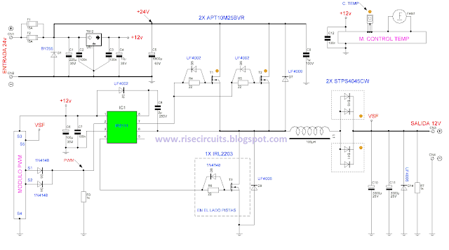
24V to 12V 400W DC Inverter Circuit

24V to 12V 400W DC Inverter Circuit Diagram
24V to 12V 400W DC Inverter Circuit

24V to 12V 20A 400W DC to DC Inverter. Does little to change my PV system 12v 24v me the problem arose of what to do with investors who already had 12V. I was looking for a pattern online and found several schemes with linear regulators 20A, this solution although quite simple, due to the huge losses they have is not advisable. Ideally, a converter switched, high-performance. At the end I found nothing I liked and decided to design my own. Circuit characteristics: Output current: 20A at 12V (15A continuous and 30A Momentary), Input voltage: 18 to 30V DC, Output voltage: 5 to 20V, Operating Frequency: 70kHz, Effectiveness: 95%, 400W maximum power, Protections: Above current (30A) in the F1 circuit, D1 and F1 polarity in the circuit.
Continue Reading..

Tuesday, September 10, 2013

An LCD Clock Kit Suitable for Beginners with Open Source Arduino Firmware

Simpleclock is an easy to assemble attractive 4-digit 7-segment LED display clock with temperature and alarm function. It is available in three display colors: Red, Blue and White. It comes as a kit of through-the-hole parts and can be soldered by any person with basic soldering experience. An attractive acrylic stand is included.

Continue Reading..

Thursday, September 5, 2013

2 4GHz WiFi ISM Band Scanner Description and Schematic Part 1

Have you ever wondered exactly what is going on in the 2.4GHz WiFi and ISM band around your house. What channel is it best to set your wireless router to? Why are you getting such poor performance across your WiFi network? Is your neighbour on the same frequency?

Just what is out there? This neat little gadget will sniff the airwaves and give you a graph of the signal strength vs frequency across the entire band. It connects to your computer by USB 2.0 and with the companion Windows software you can display the spectrum or save the raw data to an Excel compatible file for some more number crunching.

2.4GHz WiFi & ISM Band Scanner

It uses just two significant components, a radio module from Cypress Semiconductor and a PIC microcontroller from Microchip. Total cost to build it should be less than US$30.

The 2.4GHz Band

The 2.4GHz ISM (Industrial Scientific Medical) band is often called the WiFi band because it is used for WiFi networking (ie, 802.11 b/g/n). This band is unlicensed, meaning that you and anyone can transmit on it. As a result it has been used by a multitude of products including video transmitters, portable telephones, Bluetooth devices, wireless keyboards, toys and so on. Because you cannot see what is going in the band on you can experience strange behaviour from your wireless gadget. All of a sudden your wireless keyboard skips characters, is it because someone is using a portable phone on the same frequency?

The biggest victim is WiFi networking. This needs a lot of bandwidth, is always transmitting and is sensitive to interference. This is why people often cannot get a decent range from their wireless network and give up in disgust.

This scanner will draw a graph on your computer screen showing you the activity across the band and indicate the best frequencies to use. If you use a laptop you can also wander around and identify the culprits that are clogging the airwaves.

How It Works

Internally the scanner is very simple. It just contains a radio receiver and a microcontroller…

2.4GHz WiFi & ISM Band Scanner

The radio receiver is the Cypress CYWUSB6935 Radio SoC (System on a Chip). This is a complete low power radio transmitter/receiver chip for the 2.4GHz band and is controlled by a microcontroller over a synchronous serial (SPI) interface. The microcontroller can write to various registers in the chip to set things like operating frequency and can read other registers to retrieve data from the chip.

This chip is designed to operate over the 2.4GHz band and has the ability to listen on a frequency for any other devices that may be already using the frequency. This is to help the microcontroller select a suitably free frequency before transmitting. The chip reports the signal level as a number typically up to 30, with zero representing no signal. We use this facility in this project - simply put, the microcontroller instructs the module to step to a frequency and measure the signal level at that frequency, when done it steps the chip to the next frequency and instructs it to measure the signal level there. And so on, right across the band.

We actually do not use the transmit/receive function, which is normally the chips main purpose in life.

The microcontroller used in this project is the Microchip PIC18F2550 which integrates the complete USB 2.0 functionality. The microcontroller sets the radio chip to a frequency, reads the signal level from the chip, stores the value in its internal memory and steps on to the next frequency. This continues until the complete 2.4GHz band is covered. The 18F2550 then sends the data off to your computer using USB and your computer, using custom software, displays the resultant spectrum.

Physically the scanner is just a small box hanging on the end of a USB cable.

The Circuit

The circuit is the simplest part of this project. Click on the image or go to the download section at the bottom of this page for a full scale drawing.
2.4GHz WiFi & ISM Band Scanner Circuit Diagram

2.4GHz WiFi & ISM Band Scanner

The PIC 18F2550 microcontroller is a 28 pin part with a built in USB 2.0 interface. As mentioned before, the chip integrates everything connected with the USB including a 3.3V regulator, memory buffers and the USB transceiver. All that you need to do is to connect the USB cable to pins 15 and 16 of the chip and place a capacitor on pin 14 to help smooth the inbuilt 3.3V supply.

The clock for the microcontroller is derived from the 20MHz crystal with the two 15pF capacitors providing the correct loading for the crystal. Internally within the 18F2550 the 20MHz is divided by 5 to give 4MHz and then used to synchronise a phase locked loop (PLL) oscillator running at 48MHz. This is the main clock used within the microcontroller and is used to drive both the USB interface and the CPU. Running at 48MHz this is a speedy little chip so we do not have any issues with performance.

The ISCP connector is there so that I could reprogram the 18F2550 without pulling it out of its socket. It is mostly used for prototyping so you can leave it out if you want. Note that the 10K resistor on pin 1 of the 18F2550 is still needed to pull the reset line high.

Power for the circuit is drawn from the +5V supplied by the host computer on the USB cable. The whole circuit only draws a few tens of milliamps so it is not a significant load. This 5V is dropped to about 3V by three 1N4001 diodes to provide power for the Cypress CYWUSB6935 chip which is mounted on a small PCB (the CYWM6935 module). Each diode will drop about 0.7V resulting in a total voltage drop of about 2V. This is a crude way to derive a 3V supply but it is low cost and does the job without any hassles.

The CYWUSB6935 chip has protective diodes on its inputs, which clamp the signal line to its power supply (3V). This means that we can drive it with 5V signals from the microcontroller with series resistors to limit the current. This is the purpose of the 3.3K resistors, they limit the current in the clamping diodes to less than a milliamp when the PICs output goes to 5V.

CYWM6935 Module

The CYWUSB6935 chip comes in a tiny package designed for machine assembly and is virtually impossible for a mortal wielding a soldering iron to solder. Fortunately Cypress have assembled it into the CYWM6935 module along with two aerials, a crystal and a few capacitors. The connector used in the module is still rather tiny and non standard (or rather it does not use the 0.1" grid that we know and love), but it can be soldered to. For details of the CYMUSB6935 chip and CYWM6935 module go to here.

2.4GHz WiFi & ISM Band Scanner Circuit Diagram
Parts Listing
  •     1 x Microchip PIC18F2550-I/SP microcontroller programmed with the firmware available in the download section at the bottom of this page.
  •     1 x Cypress CYWM6935 radio module,
  •     1 x 20MHz crystal
  •     3 x 1N4001 silicon diodes
  •     4 x 3.3K resistors (quarter or half watt)
  •     1 x 10K resistor (quarter or half watt)
  •     2 x 15pF ceramic capacitors
  •     1 x 100nF multilayer ceramic capacitor 1 x 220nF polyester capacitor
  •     1 x 100uF electrolytic capacitor (6V or higher)
  •     1 x 28 pin IC socket
  •     1 x USB cable with a type A connector on one end
  •     1 x UB5 jiffy box

    Continue Reading..